Table of Contents
- Introduction
- About the Device
- Inter-Device Communication
- Reversing the Android App
- Reversing the Hardware
- Dumping the EEPROM
- Decapping Proprietary Chips
- SEM Imaging of Decapped Chips
Introduction
This past semester I’ve been working on a directed study at my university with Prof. Wil Robertson reverse engineering embedded devices. After a couple of months looking at a passport scanner, one of my friends jokingly suggested I hack a Furby, the notoriously annoying toy of late 1990s fame. Everyone laughed, and we all moved on with our lives.
However, the joke didn’t stop there. Within two weeks, this same friend said they had a present for me. And that’s how I started reverse engineering a Furby.
About the Device

A Furby is an evil robotic children’s toy wrapped in colored fur. Besides speaking its own gibberish-like language called Furbish, a variety of sensors and buttons allow it to react to different kinds of stimuli.
Since its original debut in 1998, the Furby apparently received a number of upgrades and new features. The specific model I looked at was from 2012, which supported communication between devices, sported LCD eyes, and even came with a mobile app.
Inter-Device Communication
As mentioned above, one feature of the 2012 version was the toy’s ability to communicate with other Furbys as well as the mobile app. However, after some investigation I realized that it didn’t use Bluetooth, RF, or any other common wireless protocols. Instead, a look at the official Hasbro Furby FAQ told a more interesting story:
Q. There is a high pitched tone coming from Furby and/or my iOS device.
A. The noise you are hearing is how Furby communicates with the mobile device and other Furbys. Some people may hear it, others will not. Some animals may also hear the noise. Don’t worry, the tone will not cause any harm to people or animals.
Digging into this lead, I learned that Furbys in fact perform inter-device communication with an audio protocol that encodes data into bursts of high-pitch frequencies. That is, devices communicate with one another via high-pitch sound waves with a speaker and microphone. #badBIOS anyone?
This was easily confirmed by use of the mobile app which emitted a modulated sound similar to the mosquito tone whenever an item or command was sent to the Furby. The toy would also respond with a similar sound which was recorded by the phone’s microphone and decoded by the app.
Upon searching, I learned that other individuals had performed a bit of prior work in analyzing this protocol. Notably, the GitHub project Hacksby appears to have successfully reverse engineered the packet specification, developed scripts to encode and decode data, and compiled a fairly complete database of events understood by the Furby.
Reversing the Android App
Since the open source database of events is not currently complete, I decided to spend a few minutes looking at the Android app to identify how it performed its audio decoding.
After grabbing the .apk via APK Downloader, it was simple work to get to the app’s juicy bits:
$ unzip -q com.hasbro.furby.apk
$ d2j-dex2jar.sh classes.dex
dex2jar classes.dex -> classes-dex2jar.jar
$
Using jd-gui, I then decompiled classes-dex2jar.jar into a set of .java source files. I skimmed through the source files of a few app features that utilized the communication protocol (e.g., Deli, Pantry, Translator) and noticed a few calls to methods named sendComAirCmd().
Each method accepted an integer as input, which was spliced and passed to objects created from the generalplus.com.GPLib.ComAirWrapper class:
private void sendComAirCmd(int paramInt)
{
  Logger.log(Deli.TAG, "sent command: " + paramInt);
  Integer localInteger1 = Integer.valueOf(paramInt);
  int i = 0x1F & localInteger1.intValue() >> 5;
  int j = 32 + (0x1F & localInteger1.intValue());
  ComAirWrapper.ComAirCommand[] arrayOfComAirCommand = new ComAirWrapper.ComAirCommand[2];
  ComAirWrapper localComAirWrapper1 = this.comairWrapper;
  localComAirWrapper1.getClass();
  arrayOfComAirCommand[0] = new ComAirWrapper.ComAirCommand(localComAirWrapper1, i, 0.5F);
  ComAirWrapper localComAirWrapper2 = this.comairWrapper;
  localComAirWrapper2.getClass();
  arrayOfComAirCommand[1] = new ComAirWrapper.ComAirCommand(localComAirWrapper2, j, 0.0F);
The name generalplus appears to identify the Taiwanese company General Plus, which “engage[s] in the research, development, design, testing and sales of high quality, high value-added consumer integrated circuits (ICs).” I was unable to find any public information about the GPLib/ComAir library. However, a thread on /g/ from 2012 appears to have made some steps towards identifying the General Plus chip, among others.
The source code at generalplus/com/GPLib/ComAirWrapper.java defined a number of methods providing wrapper functionality around encoding and decoding data, though none of the functionality itself. Continuing to dig, I found the file libGPLibComAir.so:
$ file lib/armeabi/libGPLibComAir.so
lib/armeabi/libGPLibComAir.so: ELF 32-bit LSB shared object, ARM, version 1 (SYSV), dynamically linked, stripped
Quick analysis on the binary showed that this was likely the code I had been looking for:
$ nm -D lib/armeabi/libGPLibComAir.so | grep -i -e encode -e decode -e command
0000787d T ComAir_GetCommand
00004231 T Java_generalplus_com_GPLib_ComAirWrapper_Decode
000045e9 T Java_generalplus_com_GPLib_ComAirWrapper_GenerateComAirCommand
00004585 T Java_generalplus_com_GPLib_ComAirWrapper_GetComAirDecodeMode
000045c9 T Java_generalplus_com_GPLib_ComAirWrapper_GetComAirEncodeMode
00004561 T Java_generalplus_com_GPLib_ComAirWrapper_SetComAirDecodeMode
000045a5 T Java_generalplus_com_GPLib_ComAirWrapper_SetComAirEncodeMode
000041f1 T Java_generalplus_com_GPLib_ComAirWrapper_StartComAirDecode
00004211 T Java_generalplus_com_GPLib_ComAirWrapper_StopComAirDecode
00005af5 T _Z13DecodeRegCodePhP15tagCustomerInfo
000058cd T _Z13EncodeRegCodethPh
00004f3d T _ZN12C_ComAirCore12DecodeBufferEPsi
00004c41 T _ZN12C_ComAirCore13GetDecodeModeEv
00004ec9 T _ZN12C_ComAirCore13GetDecodeSizeEv
00004b69 T _ZN12C_ComAirCore13SetDecodeModeE16eAudioDecodeMode
000050a1 T _ZN12C_ComAirCore16SetPlaySoundBuffEP19S_ComAirCommand_Tag
00004e05 T _ZN12C_ComAirCore6DecodeEPsi
00005445 T _ZN15C_ComAirEncoder10SetPinCodeEs
00005411 T _ZN15C_ComAirEncoder11GetiDfValueEv
0000547d T _ZN15C_ComAirEncoder11PlayCommandEi
000053fd T _ZN15C_ComAirEncoder11SetiDfValueEi
00005465 T _ZN15C_ComAirEncoder12IsCmdPlayingEv
0000588d T _ZN15C_ComAirEncoder13GetComAirDataEPPcRi
000053c9 T _ZN15C_ComAirEncoder13GetEncodeModeEv
000053b5 T _ZN15C_ComAirEncoder13SetEncodeModeE16eAudioEncodeMode
000053ed T _ZN15C_ComAirEncoder14GetCentralFreqEv
00005379 T _ZN15C_ComAirEncoder14ReleasePlayersEv
000053d9 T _ZN15C_ComAirEncoder14SetCentralFreqEi
000056c1 T _ZN15C_ComAirEncoder15GenComAirBufferEiPiPs
00005435 T _ZN15C_ComAirEncoder15GetWaveFormTypeEv
000054bd T _ZN15C_ComAirEncoder15PlayCommandListEiP20tagComAirCommandList
00005421 T _ZN15C_ComAirEncoder15SetWaveFormTypeEi
00005645 T _ZN15C_ComAirEncoder17PlayComAirCommandEif
00005755 T _ZN15C_ComAirEncoder24FillWavInfoAndPlayBufferEiPsf
00005369 T _ZN15C_ComAirEncoder4InitEv
000051f9 T _ZN15C_ComAirEncoderC1Ev
000050b9 T _ZN15C_ComAirEncoderC2Ev
00005351 T _ZN15C_ComAirEncoderD1Ev
00005339 T _ZN15C_ComAirEncoderD2Ev
I loaded the binary in IDA Pro and quickly confirmed my thought. The method generalplus.com.GPLib.ComAirWrapper.Decode() decompiled to the following function:
unsigned int __fastcall Java_generalplus_com_GPLib_ComAirWrapper_Decode(int a1, int a2, int a3)
{
  int v3; // ST0C_4@1
  int v4; // ST04_4@1
  int v5; // ST1C_4@1
  const void *v6; // ST18_4@1
  unsigned int v7; // ST14_4@1

  v3 = a1;
  v4 = a3;
  v5 = _JNIEnv::GetArrayLength();
  v6 = (const void *)_JNIEnv::GetShortArrayElements(v3, v4, 0);
  v7 = C_ComAirCore::DecodeBuffer((int)&unk_10EB0, v6, v5);
  _JNIEnv::ReleaseShortArrayElements(v3);
  return v7;
}
Within C_ComAirCore::DecodeBuffer() resided a looping call to ComAir_DecFrameProc() which appeared to be referencing some table of phase coefficients:
int __fastcall ComAir_DecFrameProc(int a1, int a2)
{
  int v2; // r5@1
  signed int v3; // r4@1
  int v4; // r0@3
  int v5; // r3@5
  signed int v6; // r2@5

  v2 = a1;
  v3 = 0x40;
  if ( ComAir_Rate_Mode != 1 )
  {
    v3 = 0x80;
    if ( ComAir_Rate_Mode == 2 )
      v3 = 0x20;
  }
  v4 = (a2 << 0xC) / 0x64;   if ( v4 > (signed int)&PHASE_COEF[0x157F] )
    v4 = (int)&PHASE_COEF[0x157F];
  v5 = v2;
  v6 = 0;
  do
  {
    ++v6;
    *(_WORD *)v5 = (unsigned int)(*(_WORD *)v5 * v4) >> 0x10;
    v5 += 2;
  }
  while ( v3 > v6 );
  ComAirDec();
  return ComAir_GetCommand();
}
Near the end of the function was a call to the very large function ComAirDec(), which likely was decompiled with the incorrect number of arguments and performed the bulk of the audio decoding process. Data was transformed and parsed, and a number of symbols apparently associated with frequency-shift keying were referenced.
Itching to continue onto reverse engineering the hardware, I began disassembling the device.
Reversing the Hardware
Actually disassembling the Furby itself proved more difficult than expected due to the form factor of the toy and number of hidden screws. Since various tear-downs of the hardware are already available online, let’s just skip ahead to extracting juicy secrets from the device.
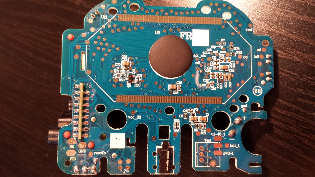
The heart of the Furby lies in the following two-piece circuit board:
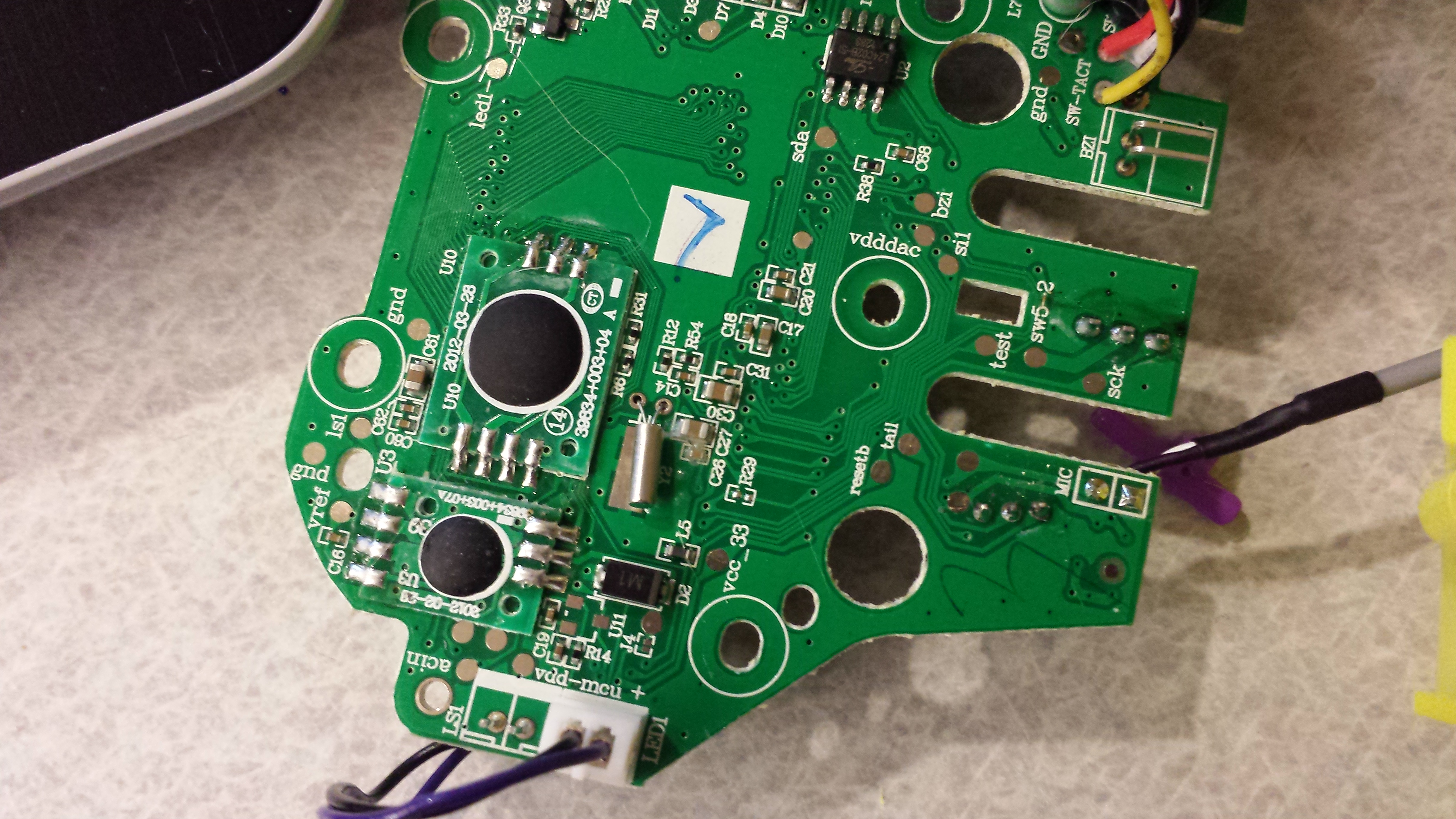
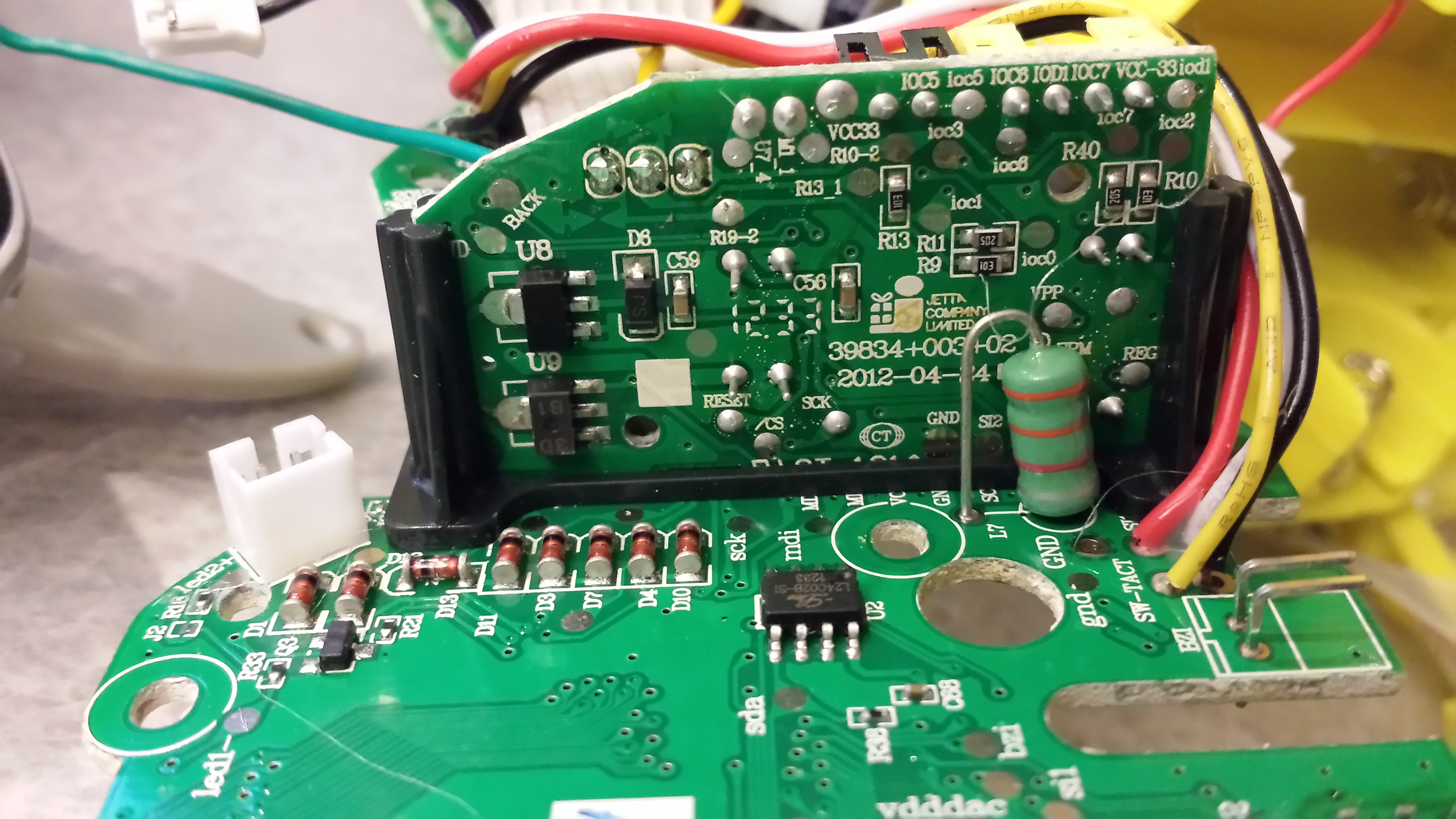
Thanks to another friend, I also had access to a second Furby 2012 model, this time the French version. Although the circuit boards of both devices were incredibly similar, differences did exist, most notably in the layout of the right-hand daughterboard. Additionally, the EEPROM chip (U2 on the board) was branded as Shenzen LIZE on the U.S. version, the French version was branded ATMEL:
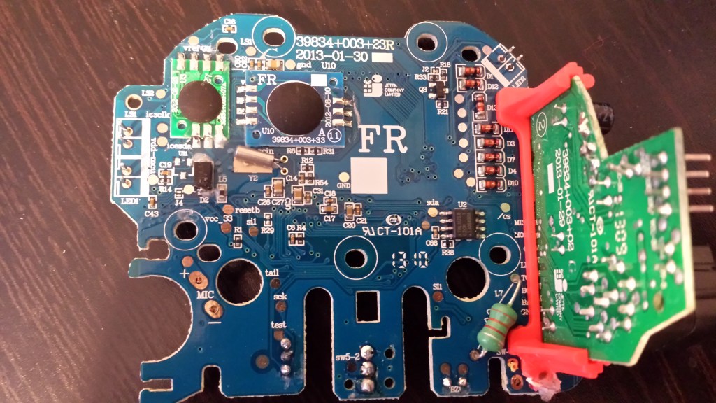
The first feature I noticed about the boards was the fact that a number of chips were hidden by a thick blob of epoxy. This is likely meant to thwart reverse engineers, as many of the important chips on the Furby are actually proprietary and designed (or at least contracted for development) by Hasbro. This is a standard PCB assembly technique known as “chip-on-board” or “direct chip attachment,” though it proves harder to identify the chips due to the lack of markings. However, one may still simply inspect the traces connected to the chip and infer its functionality from there.
For now, let’s start with something more accessible and dump the exposed EEPROM.
Dumping the EEPROM
The EEPROM chip on the French version Furby is fairly standard and may be easily identified by its form and markings:

By googling the markings, we find the datasheet and learn that it is a 24Cxx family EEPROM chip manufactured by ATMEL. This particular chip provides 2048 bits of memory (256 bytes), speaks I2C, and offers a write protect pin to prevent accidental data corruption. The chip on the U.S. version Furby has similar specs but is marked L24C02B-SI and manufactured by Shenzen LIZE.
Using the same technique as on my Withings WS-30 project, I used a heat gun to desolder the chip from the board. Note that this MUST be done in a well-ventilated area. Intense, direct heat will likely scorch the board and release horrible chemicals into the air.

Unlike my Withings WS-30 project, however, I no longer had access to an ISP programmer and would need to wire the EEPROM manually. I chose to use my Arduino Duemilanove since it provides an I2C interface and accompanying libraries for easy development.
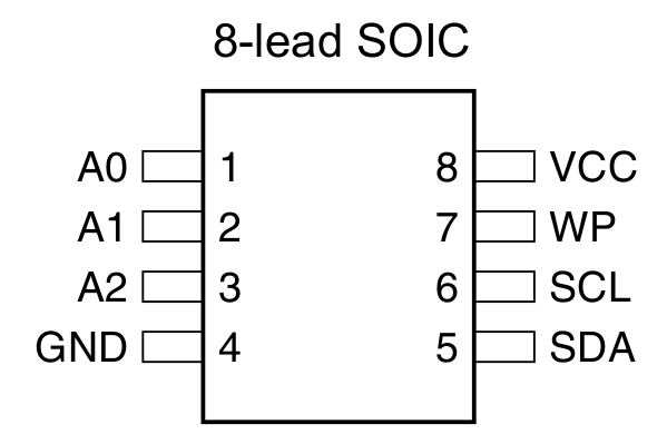
Referencing the datasheet, we find that there are eight total pins to deal with. Pins 1-3 (A0, A1, A2) are device address input pins and are used to assign a unique identifier to the chip. Since multiple EEPROM chips may be wired in parallel, a method must be used to identify which chip a controller wishes to speak with. By pulling the A0, A1, and A2 pins high or low, a 3-bit number is formed that uniquely identifies the chip. Since we only have one EEPROM, we can simply tie all three to ground. Likewise, pin 4 (GND) is also connected to ground.
Pins 5 and 6 (SDA, SCL) designate the data and clock pins on the chip, respectively. These pins are what give “Two Wire Interface” (TWI) its name, as full communication may be achieved with just these two lines. SDA provides bi-directional serial data transfer, while SCL provides a clock signal.
Pin 7 (WP) is the write protect pin and provides a means to place the chip in read-only mode. Since we have no intention of writing to the chip (we only want to read the chip without corrupting its contents), we can pull this pin high (5 volts). Note that some chips provide a “negative” WP pin; that is, connecting it to ground will enable write protection and pulling it high will disable it. Pin 8 (VCC) is also connected to the same positive power source.

After some time learning the Wire library and looking at example code online, I used the following Arduino sketch to successfully dump 256 bytes of data from the French version Furby EEPROM chip:
#include <Wire.h>

#define disk1 0x50    // Address of eeprom chip

byte i2c_eeprom_read_byte( int deviceaddress, unsigned int eeaddress ) {
    byte rdata = 0x11;
    Wire.beginTransmission(deviceaddress);
//    Wire.write((int)(eeaddress >> 8)); // MSB
    Wire.write((int)(eeaddress & 0xFF)); // LSB
    Wire.endTransmission();
    Wire.requestFrom(deviceaddress,1);
    if (Wire.available()) rdata = Wire.read();
    return rdata;

}

void setup(void)
{
  Serial.begin(9600);
  Wire.begin();

  unsigned int i, j;
  unsigned char b;

  for ( i = 0; i < 16; i++ )
  {
    for ( j = 0; j < 16; j++ )
    {
      b = i2c_eeprom_read_byte(disk1, (i * 16) + j);
      if ( (b & 0xf0) == 0 )
        Serial.print("0");
      Serial.print(b, HEX);
      Serial.print(" ");
    }
    Serial.println();
  }

}

void loop(){}
Note that unlike most code examples online, the “MSB” line of code within i2c_eeprom_read_byte() is commented out. Since our EEPROM chip is only 256 bytes large, we are only using 8-bit memory addressing, hence using a single byte. Larger memory capacities require use of larger address spaces (9 bits, 10 bits, so on) which require two bytes to accompany all necessary address bits.
Upon running the sketch, we are presented with the following output:
2F 64 00 00 00 00 5A EB 2F 64 00 00 00 00 5A EB
00 00 00 00 00 00 00 00 00 00 00 00 00 00 00 00
05 00 00 04 00 00 02 18 05 00 00 04 00 00 02 18
0F 00 00 00 00 00 18 18 0F 00 00 00 00 00 18 18
00 00 00 00 00 00 00 00 00 00 00 00 00 00 00 00
00 00 00 00 00 00 00 00 00 00 00 00 00 00 00 00
00 00 00 00 00 00 00 00 00 00 00 00 00 00 00 00
00 00 00 00 00 00 00 00 00 00 00 00 00 00 00 00
00 00 00 00 00 00 00 00 00 00 00 00 00 00 00 00
00 00 00 00 00 00 00 00 00 00 00 00 00 00 00 00
00 00 00 00 00 00 00 00 00 00 00 00 00 00 00 00
00 00 00 00 00 00 00 00 00 00 00 00 00 00 00 00
00 00 00 00 00 00 00 00 00 00 00 00 00 00 00 00
00 00 00 00 00 00 00 00 00 00 00 00 00 00 00 00
00 00 00 00 00 00 00 00 00 00 00 00 00 00 00 00
00 00 00 00 00 00 00 00 00 00 00 00 00 00 00 F8
Unfortunately, without much guidance or further analysis of the hardware (perhaps at runtime), it is difficult to make sense of this data. By watching the contents change over time or in response to specific events, it may be possible to gain a better understanding of these few bytes.
Decapping Proprietary Chips
With few other interesting chips freely available to probe, I turned my focus to the proprietary chips hidden by epoxy. Having seen a number of online resources showcase the fun that is chip decapping, I had the urge to try it myself. Additionally, the use of corrosive acid might just solve the issue of the epoxy in itself.
Luckily, with the assistance and guidance of my Chemistry professor Dr. Geoffrey Davies, I was able to utilize the lab resources of my university and decap chips in a proper and safe manner.
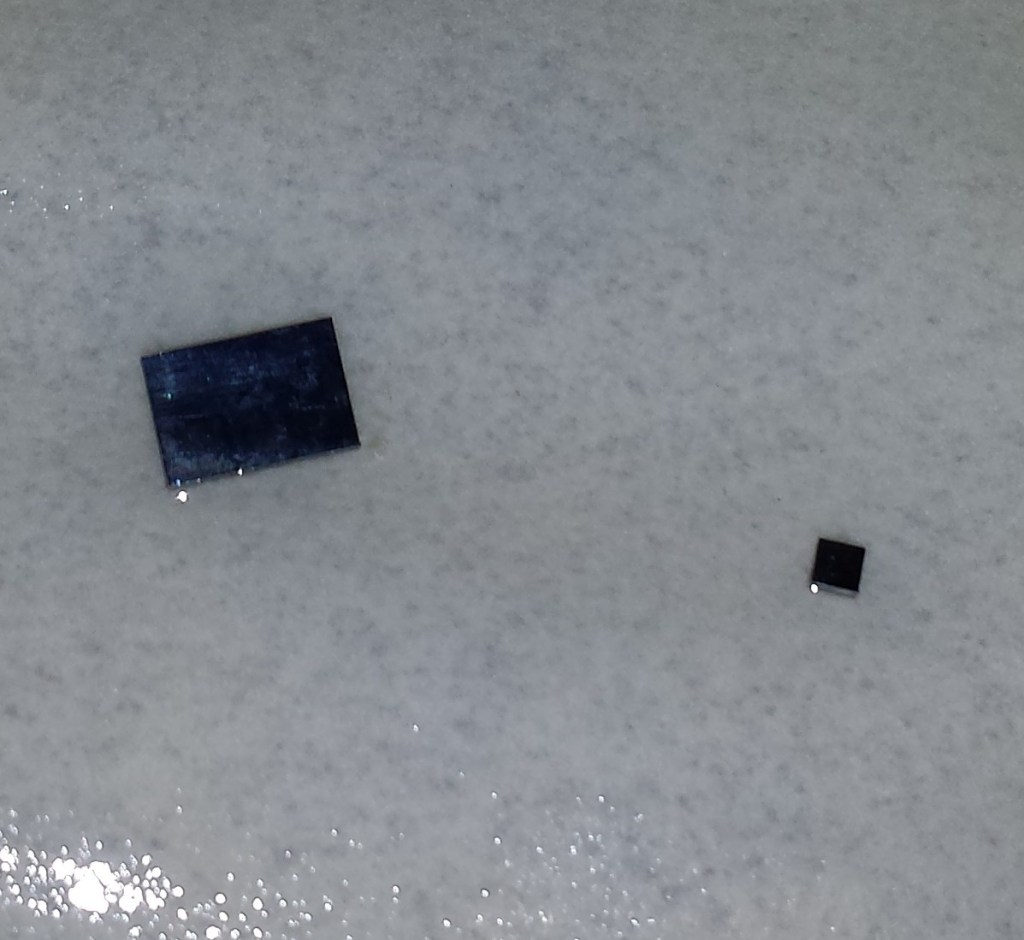
First, I isolated the three chips I wanted to decap (henceforth referenced as tiny, medium, and large) by desoldering their individual boards from the main circuit board. Since the large chip was directly connected to the underside of the board, I simply took a pair of sheers and cut around it.
Each chip was placed in its own beaker of 70% nitric acid (HNO3) on a hot plate at 68°C. Great care was taken to ensure that absolutely no amount of HNO3 came in contact with skin or was accidentally consumed. The entire experiment took place in a fume hood which ensured that the toxic nitrogen dioxide (NO2) gas produced by the reaction was safely evacuated and not breathed in.

Each sample took a different amount of time to fully decompose the epoxy, circuit board, and chip casing depending on its size. Since I was working with a lower concentration nitric acid than professionals typically use (red/white fuming nitric acid is generally preferred), the overall process took between 1-3 hours.
After each chip had been fully exposed and any leftover debris removed, I removed the beakers from the hot plate, let cool, and decanted the remaining nitric acid into a waste collection beaker, leaving the decapped chips behind. A small amount of distilled water was then added to each beaker and the entirety of it poured onto filter paper. After rinsing each sample one or two more times with distilled water, the sample was then rinsed with acetone two or three times.
The large chip took the longest to finish simply due to the size of the attached circuit board fragment. About 2.5 hours in, the underside of the chip had been exposed, though the epoxy blob had still not been entirely decomposed. At this point, the bonding wires for the chip (guessed to be a microcontroller) were still visible and intact:

About thirty minutes later and with the addition of more nitric acid, all three samples were cleaned and ready for imaging:

SEM Imaging of Decapped Chips
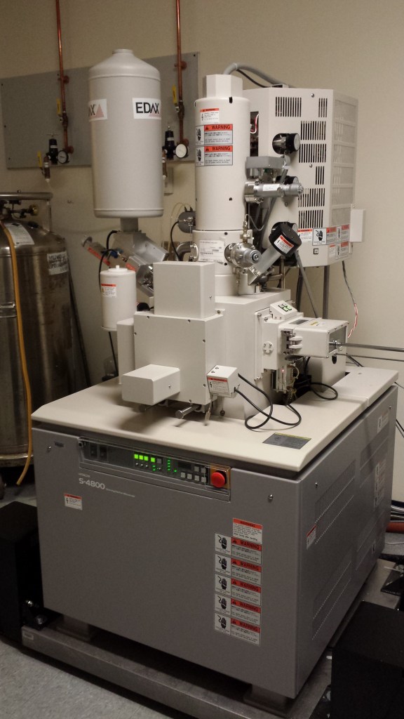
The final step was to take high resolution images of each chip to learn more about its design and identify any potential manufacturer markings. Once again, I leveraged university resources and was able to make use of a Hitachi S-4800 scanning electron microscope (SEM) with great thanks to Dr. William Fowle.
Each decapped chip was placed on a double-sided adhesive attached to a sample viewing plate. A few initial experimental SEM images were taken; however a number of artifacts were present that severely affected the image quality.
To counter this, a small amount of colloidal graphite paint was added around the edges of each chip to provide a pathway to ground for the electrons. Additionally, the viewing plate was treated in a sputter coater machine where each chip was coated with 4.5nm of palladium to create a more conductive surface.
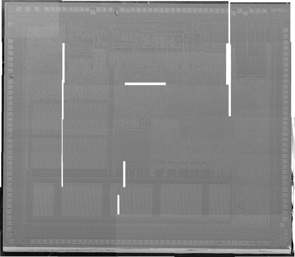
After treatment, the samples were placed back in the SEM and imaged with greater success. Each chip was imaged in pieces, and each individual image was stitched together to form a single large, high resolution picture. The small and large chip overview images were shot at 5.0kV at 150x magnification, while the medium chip overview image was shot at 5.0kV at 30x magnification:
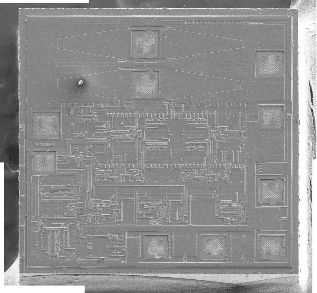
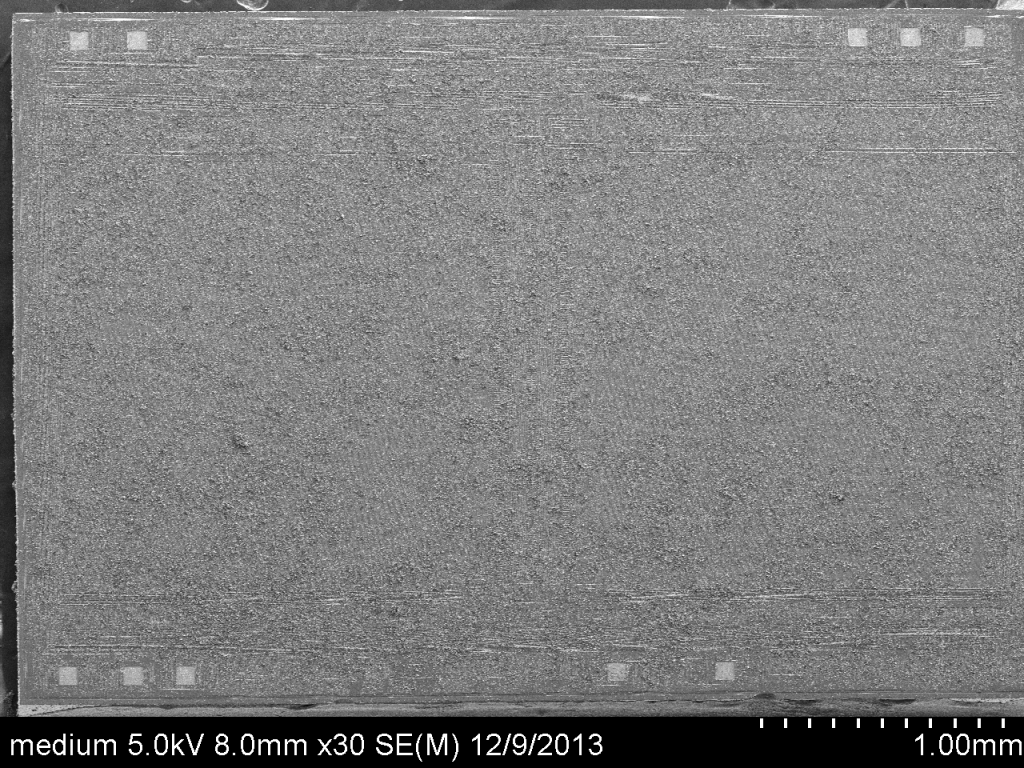
Unfortunately, as can be seen in the image above, the medium chip did not appear to have cleaned completely in its nitric acid bath. Although it is believed to be a memory storage device of some sort (by looking at optical images), it is impossible to discern any finer details from the SEM image.
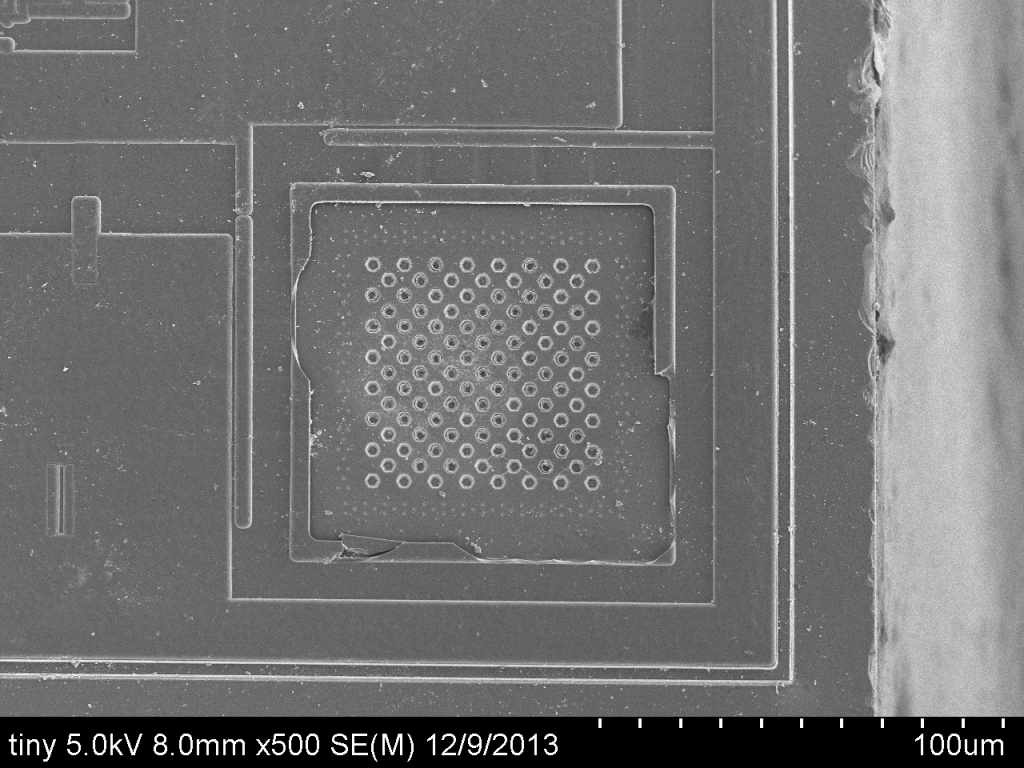
A number of interesting features were found during the imaging process. The marking “GHG554” may be clearly seen directly west on the small chip. Additionally, in similar font face, the marking “GFI392” may be seen on the south-east corner of the large chip:

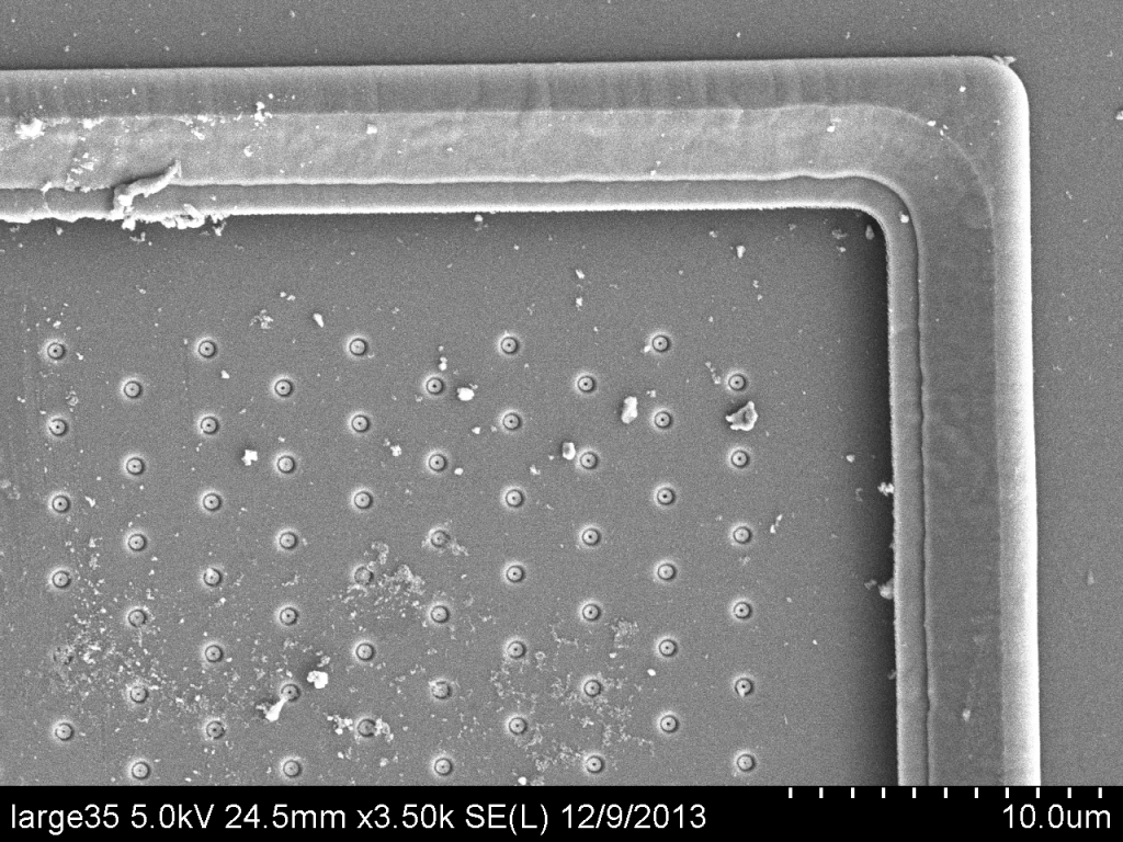
Higher zoom images were also taken of generally interesting topology on the chips. For instance, the following two images show what looks like a “cheese grater” feature on both the small and large chips:
If you are familiar with of these chips or any their features, feedback would be greatly appreciated.
EDIT: According to cpldcpu, thebobfoster, and Thilo, the “cheese grater” structures are likely bond pads.
Additional images taken throughout this project are available at: http://www.flickr.com/photos/mncoppola/
Tremendous thanks go out to the following people for their guidance and donation of time and resources towards this project:
- Prof. Wil Robertson – College of Computer and Information Science @ NEU
- Dr. Geoffrey Davies – Dept. of Chemistry & Chemical Biology @ NEU
- Dr. William Fowle – Nanomaterials Instrumentation Facility @ NEU
- Molly White
- Kaylie DeHart

34 responses to “Reverse Engineering a Furby”
Wow, those SEM photos are really, really cool! I can’t believe how detailed the images are. Great job!
Thanks!
I can’t destroy my $200+ furby 2012 to reprogram it…
[…] via Hacker News https://poppopret.org/2013/12/18/reverse-engineering-a-furby/ […]
You should try a high resolution optical microscope to look at the chips. The integrated circuits are usually capped with a relatively thick dielectric layer (usually silicon nitride), which is transparant to light, but can not be imaged very well with the SEM. Capping it with Pd does get rid of charging effects, but covers all the underlying structure. If this chip was made using CMP, you will not get a lot of structure to image that way.
However, from what I see, these look like std. logic cell designs. Will be very difficult to extract anything from them without a lot of work. This is not the same as people did with the 80ies NMOS chips where you could extract all the functionality manually with a reasonable amount of work. (reasonable= weeks).
Are the “cheese grater” structures part of the bond pads that have been etched away? I don’t see any other pads.
Thanks for the info! I’ll try to get hold of a high res optical microscope next time I decap a chip — hopefully it’ll allow for better images and analysis.
The bond pads suggestion makes a lot of sense, and is likely correct. I’m looking at other SEM chip images and they have similar features related to wire bonding.
Semiconductor physicist here. Those “cheese grater” structures are almost certainly bondpads. It’s been a while since I thought too much about fabrication, but I think one approach to making bond pads is to basically put a bunch of metal vias in close proximity to one another. (Think of vias as holes in the isolation material [probably SiO2 or a nitride maybe] that are filled with metal to allow for interconnects between different back-end-of-line metal layers). Doing that would give you a grid-like array of metal like you see in the images. Their placement around the periphery of the chip also suggests they might be bondpads. Their size is about right for typical bondpads as well.
As for overlayer coatings, YMMV. Sometimes nitrides are used as passivation, sometimes it is just SiO2 (which an optical microscope can see through quite nicely), and sometimes it can be something like (I believe) polyamide, which looks incredibly boring under an optical microscope. A few older technologies I’ve looked at used SiO2. More modern stuff has used coatings that are difficult to see through with optical microscopes. Again, I can’t speak for every fab process out there, so YMMV. One approach to dealing with these is to try to etch the passivation off, but that’s likely more trouble than you want to go through just to look at a bunch of stuff you won’t be able to identify. Also, almost every modern process uses some sort of CMP. What that means is that even if you can see through the passivation, you’re only likely to see a bunch of tiny metal squares. These are referred to as metal fill, and are used to help make sure the BEOL layers are even after each CMP step.
These images are really quite nice though. Decapping parts can be a real PITA sometimes, so good on you for going through the process.
I appreciate the information! As someone who is still relatively new to hardware, it’s great to receive input from someone with formal experience. I’ll keep it in mind for my next decapping project.
Before removing the ICs to be decapped from the PC board, it would be useful to note any easily identifiable pins such as power, ground, oscillator inputs and reset circuits.
> the fact that a number of chips were hidden by a thick blob of epoxy
> This is likely meant to thwart reverse engineers….
Surely this is just the normal Chip-On-Board method of reducing costs
(google it)
Nothing to do with keeping secrets.
I wasn’t aware of this assembly method — this makes more sense.
Hey, that the dies are directly bonded to the board and than filled with epoxy is not to make reverse engineering hard. It is simply a cost issue. It is way much cheaper to do it this way in mass production that to use chips with housing. Because the expansive part is the housing itself. You will see that, when you start working for a real company.
I wasn’t aware of chip-on-board assembly initially. I’ll update the post to reflect this.
BTW, the reversing would have been much easier if you would have been looked for the testing pads, which are presumably JTAG and used for end of line testing. With these testing pads, you would have complete access to the chips without destroying anything.
The IEEE standard for JTAG also provides for a CHIP ID, which might be useful to identify vendor/chip.
I haven’t been able to locate JTAG on the board, but I’ve been able to identify the chip another way. I’ll likely be doing a second writeup once I make more progress.
The microcontroller seems to be a Generalplus GPL169256A from the pad layout (https://mncoppola.files.wordpress.com/2014/01/gpl169256av14_ds.pdf). The pins ICESDA and ICECLK appear to be for debugging, according to this site: http://www.sunplusmcu.com/product/tap16.asp. Interestingly enough, the ICEEN (ICE enable) pin seems to be missing.
It might require purchasing a proprietary piece of hardware from Generalplus to probe the chip, though I’m not entirely sure currently since it’s difficult to find straightforward information about it online.
[…] Ingeniería inversa de un Furby […]
My sister reverse engineered the Furby for an art project, back in 2000 or so. She reprogrammed 400 of them into a large array that functioned as a mirror. You can find some “anatomical” drawings that she did of them here: http://alumni.media.mit.edu/~kelly/Furby/anatomy.htm
For more pics, you can google “Kelly Heaton Furby” and look at the Google Image results.
I thought you might be interested. Cheers!
Cool pics, thanks!
Might be worth having a chat to @natashenka – she reversed Tamagotchis which also use GeneralPlus chips
Good idea! Just re-read her Recon material
[…] que muestra la imagen, sino un ejemplo práctico de la aplicación de la ingeniería inversa a un Furby moderno, esos seres de juguete que hablan dos idiomas (Furby + el idioma local), escuchan, aceptan […]
Check out http://siliconpr0n.org/wiki/ for a lot more info. We’re trying to build the authoritative encyclopedia on semiconductor reverse engineering.
Great resource, I actually used the wiki when coming up with a lab procedure. :)
Oh, nice :)
I’m looking into teaching a seminar class at RPI on embedded reversing, probably this spring. We’ll be cross-posting lecture notes to the wiki; you may find them interesting :)
I poked around a bit on this wiki. This is a really great idea, and a much needed resource. I’m not much of a reverse-engineer myself, so I probably wouldn’t be of too much help, but I wish you the best of luck putting this together.
[…] https://poppopret.org/2013/12/18/reverse-engineering-a-furby/ […]
[…] Lapse jõulukingi saab nüüd ilusasti pulkadeks võtta. poppopret.org/2013/12/18/rev… […]
[…] Michael Coppola writes: […]
Hey Man, your dump saved my ass!
It turns our Furby back from the dark side :-)
Here is an original dump of a really evil Furby:
furby tmp # hexdump -vC FUREVIL.BIN
00000000 12 47 03 00 00 00 6a 73 12 47 03 00 00 00 6a 73 |.G….js.G….js|
00000010 00 00 00 00 00 00 00 00 00 00 00 00 00 00 00 00 |…………….|
00000020 29 00 00 68 00 00 06 e2 29 00 00 68 00 00 06 e2 |)..h….)..h….|
00000030 64 00 00 00 00 00 a0 f5 64 00 00 00 00 00 a0 f5 |d…….d…….|
00000040 00 00 00 00 00 00 00 00 00 00 00 00 00 00 00 00 |…………….|
00000050 00 00 00 00 00 00 00 00 00 00 00 00 00 00 00 00 |…………….|
00000060 00 00 00 00 00 00 00 00 00 00 00 00 00 00 00 00 |…………….|
00000070 00 00 00 00 00 00 00 00 00 00 00 00 00 00 00 00 |…………….|
00000080 00 00 00 00 00 00 00 00 00 00 00 00 00 00 00 00 |…………….|
00000090 00 00 00 00 00 00 00 00 00 00 00 00 00 00 00 00 |…………….|
000000a0 00 00 00 00 00 00 00 00 00 00 00 00 00 00 00 00 |…………….|
000000b0 00 00 00 00 00 00 00 00 00 00 00 00 00 00 00 00 |…………….|
000000c0 00 00 00 00 00 00 00 00 00 00 00 00 00 00 00 00 |…………….|
000000d0 00 00 00 00 00 00 00 00 00 00 00 00 00 00 00 00 |…………….|
000000e0 00 00 00 00 00 00 00 00 00 00 00 00 00 00 00 00 |…………….|
000000f0 00 00 00 00 00 00 00 00 00 00 00 00 00 00 00 f8 |…………….|
Haha, awesome. Would you mind explaining more?
I did a diff of the bytes, seems like there is still data in the same general spots in memory, just different. Here is the patch file: http://pastebin.com/Ntuts3gY
[…] Reverse Engineering a Furby […]
[…] case) to generate audio effects. However, an article from December 2013 by Michael Coppola – Reverse Engineering a Furby – demonstrates a wider interest, specifically in the inter-device protocol used by recent models, […]
https://www.facebook.com/openfurby